Top Benefits of Using Printed PCB for Your Electronic Projects
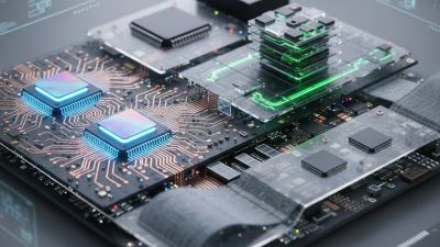
In the ever-evolving world of electronics, the choice of components can significantly impact the performance and success of a project. One critical component that stands out for its reliability and efficiency is the printed PCB (printed circuit board). As electronic designs become more complex, utilizing printed PCBs offers a multitude of benefits that can streamline the development process while enhancing the overall functionality of electronic devices.
Printed PCBs are not only cost-effective but also provide high precision in circuit design, which is essential for minimizing errors and optimizing performance. Furthermore, their compact design allows for greater flexibility in layout, enabling engineers to create more intricate and powerful electronic systems without compromising on space or functionality. This introduction to the advantages of printed PCBs opens the door to understanding why they have become the preferred choice for hobbyists and professionals alike in the realm of electronic projects.

Top Benefits of Using Printed PCB for Your Electronic Projects
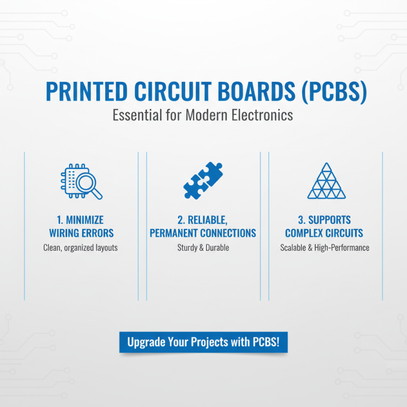
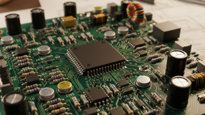
Printed circuit boards (PCBs) are essential for modern electronic projects, providing a sturdy and organized platform for components. One of the primary benefits of using printed PCBs is their ability to minimize wiring errors and create reliable connections. Unlike prototyping with breadboards, printed PCBs offer a permanent solution for electronics, ensuring that circuits remain intact over time. Additionally, they can be designed to accommodate complex circuits, making it easier to scale projects without compromising quality or performance.
When working with printed PCBs, it’s crucial to consider design and layout. Properly organizing components and traces can significantly enhance performance and reduce interference. Here are some tips:
1. **Plan Your Layout**: Before finalizing your PCB design, sketch a rough layout. Keep related components close to minimize trace lengths and reduce signal degradation.
2. **Test with Simulation Software**: Utilize PCB design software that offers simulation features. Running simulations can help identify potential problems before fabrication, saving time and resources.
3. **Choose the Right Materials**: Different projects may require specific materials based on factors like heat dissipation and electrical insulation. Selecting the right substrates can impact the lifespan and effectiveness of your PCB.
Embracing printed PCBs in your electronic projects not only enhances functionality but also significantly increases the reliability and professionalism of your designs.
Enhanced Design Flexibility: Tailoring PCBs to Specific Project Needs
When it comes to electronic projects, the design flexibility offered by printed circuit boards (PCBs) is unmatched. With the ability to tailor PCBs to meet specific project requirements, designers can optimize layout, size, and functionality. According to a report by the IPC (Association Connecting Electronics Industries), 75% of engineering teams reported enhanced customization capabilities significantly improved their product development timelines. This level of flexibility not only supports innovative designs but also allows engineers to experiment with various configurations, ensuring that the final product meets all necessary performance criteria.
Moreover, printed PCBs can be designed to accommodate specific components and functionalities without the typical constraints found in rigid PCB solutions. The adaptability of PCBs extends to both single-sided and multi-layer designs, which enables intricate circuit layouts and better space utilization. Citing a study from the Design Automation Conference, 68% of respondents indicated that using custom-designed PCBs reduced prototyping errors and accelerated the development process. This indicates that a tailored approach not only enhances performance but also improves overall project efficiency, making printed PCBs a vital asset for anyone engaged in electronic hardware development.
Cost Efficiency: Reducing Material Waste and Production Costs
Using printed PCBs in electronic projects offers significant cost efficiency, primarily by reducing material waste and production costs. Printed circuit boards are designed to optimize the layout of electronic components, ensuring that the space is utilized effectively. This thoughtful arrangement minimizes excess material that would typically be discarded in traditional circuit design processes. By adhering to specific manufacturing standards and employing advanced techniques, the production of printed PCBs ensures that each board maximizes utility while minimizing scrap.
Moreover, the economies of scale achieved through the mass production of printed PCBs contribute to a reduction in overall production costs. When manufacturers produce PCBs in larger quantities, the cost per unit decreases significantly, making it more affordable for hobbyists and businesses alike to implement these essential components into their projects. Furthermore, the integration of automated processes in PCB production minimizes labor costs and decreases the likelihood of human errors, which can lead to costly revisions or replacements. As a result, embracing printed PCBs not only streamlines the development process but also enhances the financial viability of electronic projects, making them more accessible to all creators.
Improved Performance: Higher Signal Integrity and Reduced Noise
When it comes to electronic projects, utilizing printed circuit boards (PCBs) offers significant advantages, particularly in terms of signal integrity and noise reduction. Printed PCBs are meticulously designed to organize components and routes on the board, which minimizes the distance that signals must travel. This shorter path is crucial for maintaining high signal integrity, especially at higher frequencies, where even minor interference can lead to performance degradation.
One of the most notable benefits of printed PCBs is their ability to greatly reduce electronic noise. By placing components in close proximity to each other and using controlled impedance, PCBs can effectively limit the crosstalk between traces. This controlled environment also minimizes electromagnetic interference (EMI), allowing your electronic project to operate more smoothly and efficiently.
Tips for achieving the best performance with printed PCBs include keeping the layout as compact as possible and ensuring proper grounding techniques are followed. Additionally, consider using multi-layer boards for complex circuits, as they can help isolate signals and layers, further enhancing performance. Always prioritize a clean design; cluttered layouts not only add to the noise but also complicate troubleshooting should issues arise during testing.
Scalability: Easily Transitioning from Prototypes to Mass Production
When embarking on electronic projects, scalability is a critical factor that can determine the success and efficiency of product development. Printed circuit boards (PCBs) play an essential role in this aspect, allowing creators to seamlessly transition from prototype development to mass production. The process of designing a PCB for a prototype often involves initial iterations to test functionality and design parameters. Once the final version is approved, the same designs can be easily replicated for larger scale manufacturing, minimizing the need for redesign and ensuring consistent quality across all units produced.
This smooth transition from small-scale prototypes to mass production not only saves time but also reduces costs significantly. Manufacturers can utilize automated processes to produce PCBs in bulk, ensuring that the specifications of the prototypes are met with precision in the larger batches. Furthermore, having a standardized design facilitates dynamic adjustments based on market feedback or performance testing, thereby enhancing the overall adaptability of electronic projects. This level of scalability is vital for maintaining competitiveness in a rapidly evolving tech landscape, where speed and efficiency are crucial for meeting consumer demands.
Top Benefits of Using Printed PCB for Your Electronic Projects - Scalability: Easily Transitioning from Prototypes to Mass Production
| Benefit |
Description |
Scalability Level |
Cost Efficiency |
| Rapid Prototyping |
Allows quick iterations and modifications of designs to enhance product development. |
High |
Saves costs on materials and labor during the prototype phase. |
| Design Flexibility |
Easily adjustable layouts for various applications, enhancing project adaptability. |
Medium |
Facilitates cost management by streamlining multiple design adjustments. |
| Consistent Quality |
Ensures uniformity in production, which is key for reliability in mass production. |
High |
Reduces costs tied to defects and returns by ensuring high quality. |
| Streamlined Manufacturing |
Simplifies the transition from small-scale to large-scale production processes. |
High |
Optimizes manufacturing costs through efficient production techniques. |
| Reduced Time to Market |
Accelerates the development cycle leading to quicker market entries. |
High |
Contributes to financial savings by leveraging early market capture. |
Conclusion
The article "Top Benefits of Using Printed PCB for Your Electronic Projects" highlights several key advantages of utilizing printed PCBs in electronic design and manufacturing. One prominent benefit is enhanced design flexibility, allowing engineers to tailor PCBs specifically to the needs of their projects. This customization aids in optimizing various aspects of performance, including higher signal integrity and reduced electromagnetic noise, ultimately leading to better-functioning devices.
Additionally, printed PCBs contribute to cost efficiency by reducing material waste and production expenses. Their scalability is another significant advantage, facilitating a smooth transition from prototype development to mass production without compromising quality. Lastly, the reliability and durability of printed PCBs ensure an extended lifespan for electronic devices, making them a preferred choice for modern electronic projects.