How to Design a Printed Circuit Board for Beginners in Easy Steps
The printed circuit board (PCB) is a foundational component of modern electronics, enabling the functionality of devices we rely on every day, from smartphones to medical equipment. According to a report by MarketsandMarkets, the global PCB market size is expected to reach USD 83.3 billion by 2026, growing at a CAGR of 3.9% from 2021 to 2026. This growth reflects the increasing demand for advanced electronics in various sectors, emphasizing the importance of PCB design in the manufacturing process.
For beginners venturing into the world of PCB design, understanding the basic principles and steps is crucial. The design process includes critical considerations such as layer stacking, trace width, and component placement, all of which can significantly impact the performance and reliability of the final printed circuit board. As the industry evolves, accessibility to PCB design tools and resources has improved, making it easier for novices to learn and apply PCB design techniques effectively. By following systematic steps, aspiring engineers and hobbyists can create their own printed circuit boards, contributing to the ever-expanding field of electronics.
Understanding the Basics of Printed Circuit Board (PCB) Design
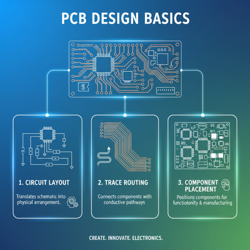
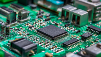
Understanding the basics of printed circuit board (PCB) design is essential for anyone looking to delve into electronics. A printed circuit board serves as the backbone of electronic devices, allowing components to connect and function together seamlessly. The fundamental elements of PCB design include circuit layouts, trace routing, and component placement. By mastering these components, beginners can create functional PCBs that meet their project's specifications.
One of the primary steps in PCB design is to develop a schematic diagram. This diagram visually represents the circuit connections and components, serving as a blueprint for the PCB layout. After defining the schematic, it's crucial to consider the physical layout of the circuit. This involves arranging components in an efficient manner to minimize interference and maintain signal integrity. Essential design rules, such as trace width and spacing, should be followed to ensure that the PCB can handle the required electrical loads without failure. As you gain confidence with these basics, you'll find that designing a PCB becomes a rewarding and creative process.
Choosing the Right PCB Materials for Your Project
When embarking on designing a printed circuit board (PCB), selecting the right materials is crucial to ensuring both functionality and longevity. Different PCB materials can significantly impact the performance, durability, and cost-effectiveness of your project. For instance, FR-4 is one of the most commonly used materials due to its excellent electrical insulating properties and suitability for a wide range of applications. According to a report from IPC, nearly 85% of PCBs are made using FR-4, primarily because it balances performance and affordability.
In addition to FR-4, it's essential to consider other material options based on your project requirements. For high-frequency applications, materials like Rogers or PTFE can reduce signal loss and improve performance. The right substrate can also influence the thermal management of the PCB, which is vital for components that dissipate heat. A study by IHS Markit reveals that improper material selection can lead to a 30% increase in failure rates in PCBs, highlighting the importance of careful material considerations.
**Tips**: Always evaluate the specific electrical and thermal requirements for your project before selecting materials. Additionally, consider the manufacturing process, as some materials may be more suited to specific fabrication techniques. Lastly, stay informed about new materials and technologies that could enhance your PCB design, as the industry is constantly evolving.
Step-by-Step Guide to PCB Layout and Design Software
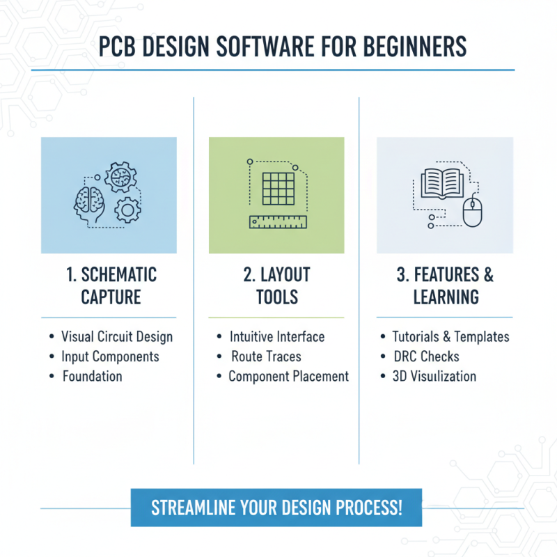
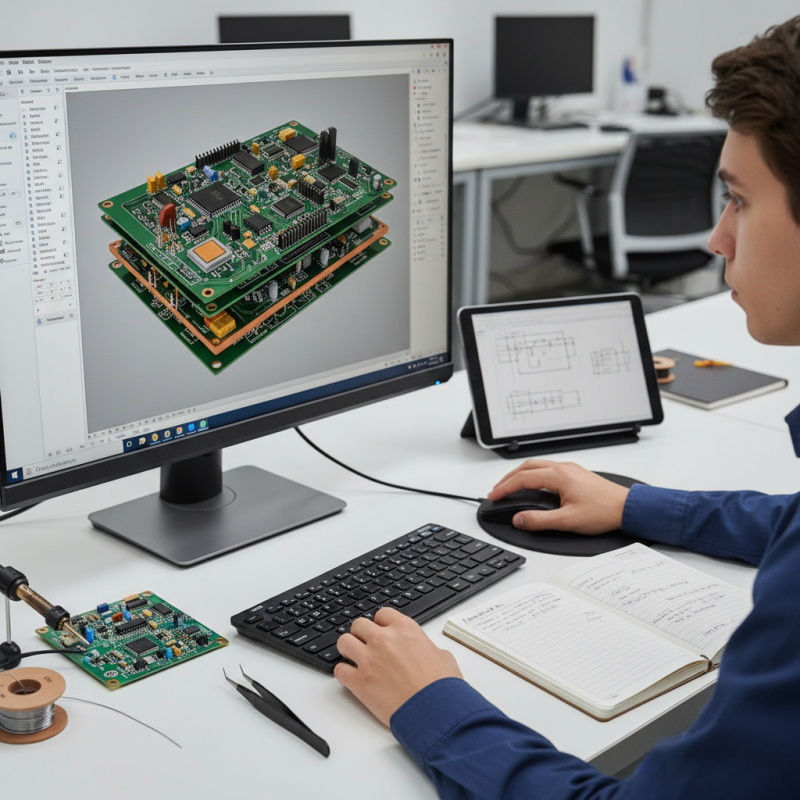
When embarking on the journey of designing a printed circuit board (PCB), understanding the software options available for PCB layout is crucial for beginners. Various design software tools offer intuitive interfaces and robust features that streamline the design process. Many programs come equipped with tutorials and templates that help users familiarize themselves with the layout procedures. Starting with basic schematic capture, beginners can input components and create a visual representation of their circuit, laying the foundation for an effective PCB design.
Once the schematic is complete, the next step involves transitioning to PCB layout. This stage often includes arranging components, routing traces, and ensuring that the design adheres to electrical and physical standards. The software typically provides design rule checks (DRC) to flag any potential issues that may arise, such as trace widths being too narrow or component placement violating spacing rules. By utilizing these built-in tools, beginners can simplify the design process and develop PCB prototypes that are reliable and ready for fabrication. Whether creating a simple project or a more complex circuit, mastering these design software tools is essential for anyone looking to produce effective PCBs.
Essential Design Rules and Common Mistakes to Avoid
When embarking on the journey of designing a printed circuit board (PCB), understanding essential design rules can significantly enhance the overall quality and functionality of your project. One critical guideline is maintaining adequate spacing between traces to prevent short circuits. A good practice is to adhere to the minimum trace width and spacing defined by the manufacturing process. This helps ensure the integrity of the electrical signals while avoiding unintended interactions between closely packed components.
Additionally, novices often overlook the importance of component placement. It is crucial to arrange components logically to minimize signal path lengths and interference. Beginners should also be aware of common mistakes, such as neglecting to account for thermal management and voltage drops. Proper heat dissipation techniques and voltage regulation can prevent circuit failures and improve longevity. By focusing on these design principles and being aware of frequent pitfalls, beginners can create efficient and reliable PCBs with confidence.
Common Mistakes in PCB Design
Finalizing Your PCB Design and Preparing for Manufacturing
Finalizing your PCB design is a crucial step that ensures the transition from concept to an actual product goes smoothly.
After you have completed your initial layout, it's important to review your design for any errors or inconsistencies.
This includes verifying component placement, checking for potential short circuits, and ensuring that traces are adequately sized
to handle the required current.
Utilize design rule checks (DRCs) offered by PCB design software
to help identify common issues that may not be readily apparent during manual reviews.
Once you are satisfied with the design, it's time to prepare for manufacturing. Generate the necessary files for production,
including Gerber files, which provide the detailed information needed for fabrication.
Ensure that you include all required documentation, such as assembly instructions and a bill of materials (BOM), to communicate
effectively with manufacturers. It's also wise to consider the specific manufacturing capabilities and limitations to make your
design compatible with their processes, which can help prevent costly revisions later on.
This final step is vital to streamline the production process
and bring your PCB design to life efficiently.