How to Design a Printed Circuit Board Effectively?
The design of a printed circuit board (PCB) plays a crucial role in modern electronics. According to a recent industry report by IPC, the global PCB market was valued at approximately $61.4 billion in 2020 and is expected to grow steadily. This growth emphasizes the increasing importance of effective PCB design in various applications. Experts like Dr. Emily Chen, a leading PCB designer, emphasize, “Design is the foundation. Flaws in a PCB can lead to catastrophic failures.”
Effective PCB design involves more than just layout. It requires understanding component placement, electrical performance, and manufacturability. A well-designed PCB minimizes errors and improves reliability. Poor design decisions can lead to costly revisions. Studies show that 45% of PCB failures are due to design mistakes. This highlights the need for meticulous attention to detail throughout the design process.
Furthermore, as technology advances, PCBs face new challenges. High-frequency signals and dense component layouts complicate designs. Designers must adapt and innovate continually. Reflecting on past designs can reveal areas for improvement. Prioritizing efficient design practices is essential for success in the PCB industry.
Understanding the Basics of Printed Circuit Board (PCB) Design
Designing a Printed Circuit Board (PCB) requires a solid understanding of its fundamentals. A PCB is an essential component for modern electronics, connecting various elements in a circuit. According to industry data, the global PCB market was valued at $61.3 billion in 2020 and is projected to grow by 4.1% annually. This demonstrates the increasing reliance on PCBs in technology.
Understanding the layout and electrical pathways is crucial. Design errors can lead to significant failures, especially in high-density applications. Reports indicate that up to 30% of PCB prototypes fail due to inadequate design. This statistic highlights the need for careful planning and thorough testing. Engineers must consider factors such as trace width, layer stack-up, and component placement.
Attention to detail is key. Mistakes like insufficient clearance can result in short circuits. Many designs overlook grounding and power distribution, which can affect performance. An effective PCB requires a balance between functionality and manufacturability. By analyzing common pitfalls and reflecting on previous designs, designers can avoid costly revisions.
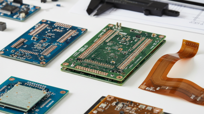
Identifying Key Components and Their Placement on PCBs
When designing a printed circuit board (PCB), component placement is crucial. A well-thought-out layout can enhance performance significantly. Begin by identifying essential components like resistors, capacitors, and microcontrollers. Consider their function and how they interact. Group related components together to minimize trace lengths. This practice helps in reducing interference and makes the overall design cleaner.
In practice, the efficiency of placement often hinges on clarity. Ensure that components are not too close to each other. This can lead to heat issues and signal disruptions. Space allows for easier soldering and assembly. Additionally, think about routing traces. Complex layouts can lead to mistakes. It's essential to have a balance between compact designs and spacious arrangements. Sometimes, less is more in PCB design.
Iterating on your design is key. Early placements may not be optimal. Review and test different configurations. Aim to improve heat dissipation and signal integrity. Feedback from prototypes can guide adjustments. Embrace mistakes as learning opportunities. This reflective process leads to better designs. Ultimately, an effective PCB requires a balance between function, space, and performance.
Choosing the Right Materials for Effective PCB Fabrication
Choosing the right materials is crucial for effective PCB fabrication. The substrate material plays a significant role in the performance of the PCB. Common choices include FR-4, polyimide, and CEM-1. Each material has unique properties that affect electrical performance and thermal stability. For high-frequency applications, specific materials are better suited.
**Tips:** Always test different substrates to find the best fit for your project. Verify thermal properties through simulation or prototyping. It’s important to consider both initial cost and long-term reliability.
Copper thickness is another critical factor. Thicker copper can handle higher currents but may complicate manufacturing. Thinner copper might be easier to work with but can lead to issues in heavy-load scenarios. Balancing these aspects requires careful analysis of your design needs.
**Tips:** Review current requirements before selecting copper thickness. Do not hesitate to consult with experts. They may provide insights that enhance your design process. Remember, the right material choice prevents issues down the line.
PCB Material Selection for Effective Fabrication
Utilizing PCB Design Software for Enhanced Efficiency
When designing a printed circuit board (PCB), utilizing PCB design software can significantly boost efficiency. These tools offer various features that simplify complex tasks. Designers can create schematics, layout components, and run simulations. This integration saves time and reduces errors. A typical software package will include automation tools, allowing for quicker adjustments and fewer manual errors.
Tips: Always start with a clear schematic. A well-defined diagram can prevent confusion later. Regularly check for design rule violations. This small step saves lots of time during the final review. Also, use layers effectively. Separate signals and power to avoid interference.
Utilizing software effectively is essential. However, many designers overlook the learning curve. While the tools are powerful, they can also be complex. Taking time to understand software features can lead to better designs. Experiment with different layouts and settings. Reflection on past mistakes can lead to improvement. Ensure every design choice aligns with project goals and constraints. This can result in a more effective PCB design process.
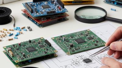
Testing and Troubleshooting Your PCB for Optimal Performance
Testing and troubleshooting your printed circuit board (PCB) is essential for ensuring optimal performance. Early detection of issues can prevent costly design revisions later. According to industry data, up to 70% of PCB failures occur in the design and manufacturing phases. Identifying these problems before production saves time and resources.
One effective tip is to perform extensive simulations before physical prototyping. Tools like finite element analysis (FEA) can predict thermal and electrical performance. Also, produce a prototype as early as possible. This allows for hands-on testing and helps catch errors that simulation might miss. Inspect for solder joint quality and verify component placement meticulously.
Another key area to focus on is signal integrity. Poor signal quality leads to instability in performance. According to reports, issues with signal integrity account for about 30% of PCB failures. Emphasizing proper layout techniques and decoupling capacitors can significantly enhance signal reliability. Check for ground loops and interference during testing. Debugging can lead to frustration. But every challenge is an opportunity for learning and improvement.