
What Is a PCB Board and How Does It Work?
A pcb board is the quiet foundation inside many electronic products. It connects components, carries electrical signals, and supports reliable assembly. You may find one in a phone, router, medical instrument, or industrial controller. Under a protective surface, copper traces form carefully planned pathways. These paths replace much of the loose wiring used in older equipment.
Understanding how a pcb board works starts with its layers. A basic board may contain a fiberglass core, copper foil, solder mask, and printed labels. More advanced designs use several copper layers to route power and high-speed signals. Components such as resistors, capacitors, processors, and connectors attach to drilled holes or surface pads. When power enters the board, traces guide current between these components. The result is a controlled circuit rather than a random collection of parts.
Small details matter. A damaged solder joint can interrupt an entire product. Excess heat may weaken materials or shorten component life. Engineers therefore review trace width, spacing, grounding, thermal paths, and manufacturing tolerances. A practical inspection might reveal uneven solder, scratched coating, or a connector that feels loose. Not every visible flaw causes failure, however. This is where testing becomes essential. Continuity checks, automated inspection, and functional testing provide stronger evidence than appearance alone. It is easy to oversimplify a pcb board as “just wiring.” That view misses its mechanical, thermal, and electrical roles. This guide explains those roles clearly, while recognizing that real designs often involve compromises, revisions, and occasional mistakes.
PCB Board Definition and Core Functions
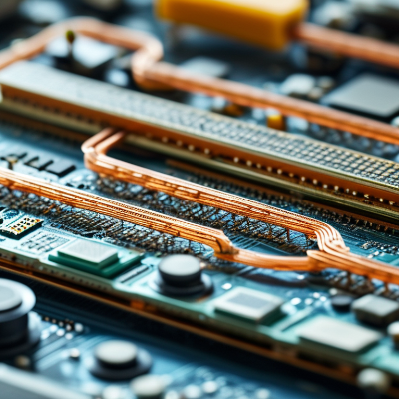
A printed circuit board, or PCB, is a rigid or flexible platform that connects electronic components through copper pathways. Those pathways, called traces, carry electrical signals and power between locations. A typical multilayer PCB contains copper layers, insulating material, drilled vias, and a protective solder mask. The visible pads provide controlled points for mounting components.
Its core functions are connection, support, routing, and heat management. Engineers place traces to control distance, impedance, and signal interference. Vias link different copper layers through small holes. The board also holds components firmly during vibration, assembly, and service. IPC-2221 design guidance emphasizes spacing, insulation, current capacity, and mechanical reliability. In practice, a narrow power trace can become dangerously hot, while poor grounding may create unstable signals. Small details matter.
Industry data shows why this structure remains important. The Global Electronics Association’s 2024 industry outlook estimated worldwide PCB production at well above 60 billion dollars annually, with demand tied to computing, vehicles, communications, and medical electronics. A 2024 market analysis by Fortune Business Insights projected continued global PCB growth through 2032. These figures reflect scale, not guaranteed quality. The common explanation, “a PCB is just a circuit holder,” is too simple. It is also a carefully engineered electrical environment. Yet even experienced designers can miss thermal stress, connector wear, or manufacturing variation. That is where testing, documented tolerances, and design review become essential.
What Is a PCB Board and How Does It Work? - PCB Board Definition and Core Functions
| Data Dimension | Typical Definition or Range | Core Function and Practical Meaning |
|---|---|---|
| Basic Definition | Printed Circuit Board (PCB) | A rigid or flexible board that mechanically supports electronic components and electrically connects them through patterned conductive paths. |
| Main Conductive Material | Copper foil | Copper forms the traces, pads, planes, and vias that carry electrical current and signals between components. |
| Common Base Material | Glass-reinforced epoxy laminate, commonly called FR-4 | The insulating laminate provides mechanical strength, dimensional stability, and electrical separation between copper layers. |
| Number of Layers | 1, 2, or multiple layers | Single-layer boards suit simple circuits, double-layer boards support more routing, and multilayer boards provide higher routing density and dedicated power or ground planes. |
| Copper Thickness | Commonly about 17 to 70 micrometres for standard designs | Thicker copper can carry higher current and improve heat spreading, while thinner copper is useful for compact signal routing and fine features. |
| Electrical Insulation | Dielectric laminate and prepreg layers | Insulating layers prevent short circuits and establish controlled spacing and impedance between adjacent conductive layers. |
| Conductive Features | Traces, pads, copper pours, and planes | These features distribute power, route signals, connect component terminals, reduce electrical resistance, and support electromagnetic control. |
| Vias | Plated holes connecting two or more copper layers | Vias transfer electrical signals and power vertically through a multilayer board. Common types include through vias, blind vias, and buried vias. |
| Component Mounting | Through-hole or surface-mount technology | Through-hole components use leads inserted into drilled holes, while surface-mount components are soldered directly onto surface pads for compact assembly. |
| Solder Mask | Protective polymer coating over most copper areas | The solder mask helps prevent solder bridges, protects copper from oxidation, and improves electrical insulation during assembly and use. |
| Component Marking | Silkscreen or other printed identification layer | Markings identify component locations, polarity, reference designators, test points, and assembly instructions. |
| Power Distribution | Power traces, copper pours, and power planes | The board delivers regulated voltage and current to components while helping control voltage drop, current density, and heat generation. |
| Signal Routing | Designed paths with controlled width, spacing, and length | Routing determines how digital, analog, high-speed, and radio-frequency signals travel between circuit elements and affects signal integrity. |
| Thermal Management | Copper areas, thermal vias, and heat-spreading structures | These features transfer heat away from components and distribute it across the board or toward external cooling structures. |
| Mechanical Support | Board outline, mounting holes, slots, and stiffeners | Mechanical features position the PCB inside an enclosure, withstand handling and vibration, and maintain alignment with connectors and other assemblies. |
| Typical Manufacturing Sequence | Imaging, etching, drilling, plating, lamination, solder-mask application, and testing | These processes create the circuit pattern, connect layers, protect the board, and verify electrical continuity and insulation. |
| Electrical Testing | Continuity and isolation checks | Testing confirms that intended connections are conductive and that unintended connections or short circuits are absent. |
| Common PCB Types | Rigid, flexible, and rigid-flex | Rigid boards provide structural strength, flexible boards bend within specified limits, and rigid-flex designs combine both characteristics in one assembly. |
| Primary Design Trade-Offs | Cost, size, layer count, current capacity, signal performance, and manufacturability | A successful PCB balances electrical, thermal, mechanical, and production requirements while maintaining reliable performance over its intended service life. |
Related Posts
-
10 Essential Tips for Understanding Circuit Boards and Their Functionality
-

Top 10 Benefits of Using PCB Boards in Electronics Manufacturing
-

How to Design a Circuit Board Efficiently in 2026?
-
Understanding PCB Production: Essential Insights for Future Electronics Innovators
-
How to Design a Printed Circuit Board for Beginners in Easy Steps
-

Top 10 Circuit Board Design Tips for Beginners and Experts