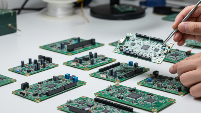
10 Circuit Board Design Tips for Global Buyers
Buying a circuit board from a global supplier requires more than comparing prices and delivery dates. Design choices affect performance, production yield, maintenance, and long-term reliability. A board that looks excellent on a screen may fail after repeated heat cycles, vibration, or moisture exposure. Small details matter.
This guide presents ten practical circuit board design tips for international buyers. It considers component availability, material selection, stack-up planning, signal integrity, thermal control, manufacturing tolerances, and inspection requirements. These factors can influence whether a prototype becomes a stable product or an expensive rework project. Supplier experience also matters. An experienced manufacturer can identify unclear specifications before fabrication begins and recommend realistic design adjustments.
Ask precise questions.
Global purchasing adds communication challenges. Different suppliers may interpret drawings, tolerances, testing standards, and revision notes differently. Clear documentation reduces that risk. Include controlled files, approved materials, acceptance criteria, and sample requirements. Request evidence, not broad promises: process certifications, inspection records, test methods, and production references can provide useful confidence.
No checklist is perfect. A design that succeeds in one climate, market, or production volume may need revision elsewhere. I have seen teams focus heavily on unit cost while overlooking connector wear, repair access, or component substitutions. Those omissions can become costly later. Thoughtful circuit board design combines engineering judgment with supplier verification. It also leaves room for honest review when assumptions prove wrong. For global buyers, that practical balance supports better decisions, clearer communication, and more dependable products.

Understanding Global Circuit Board Requirements and Standards
10 Circuit Board Design Tips for Global Buyers
Global circuit board requirements vary by destination, industry, and product risk. A board designed for one market may fail another market’s safety or environmental review. Confirm current electrical, material, and labeling rules before layout begins. Regulations change. Recheck them.
Tip 1: Define the destination markets early. Tip 2: Select materials with documented compliance evidence. Tip 3: Match insulation spacing to the target voltage and pollution environment. Tip 4: Plan for regional testing, marking, and technical documentation. Experienced engineers also review temperature, humidity, vibration, and altitude conditions. A tropical enclosure needs different protection than a dry laboratory. Tiny details matter.
Tip 5: Use recognized design and manufacturing standards for traceability. Tip 6: Control impedance with a documented stack-up. Tip 7: Keep safety-critical paths physically separated. Tip 8: Specify cleanability and moisture protection when needed. Tip 9: Require inspection records for every production batch. Tip 10: Confirm that substitute materials remain compliant. This step is often overlooked. I have seen otherwise sound designs delayed by missing supplier declarations. No checklist is perfect. Engineers should question assumptions, especially when a familiar component becomes unavailable. Independent testing can expose weak points before shipment. It also strengthens buyer confidence and supports reliable approval decisions across different regions.
Selecting Materials, Layers, and Board Specifications
For global buyers, board selection should begin with operating conditions, not a preferred material. Standard FR-4 suits many digital products, but high-temperature equipment may need high-Tg laminate. Aluminum substrates can move heat efficiently in LED and power assemblies. They are less suitable when dense routing requires many plated vias. Ask for dielectric thickness, copper weight, surface finish, and flammability rating. These details affect heat, signal loss, and assembly yield.
Layer count should follow routing and power needs. A two-layer board can control cost for simple sensors. A four-layer design often provides cleaner grounding and shorter return paths. High-speed interfaces may require controlled impedance, measured from the finished stack-up. Do not accept “standard stack-up” as a complete specification. It is too vague. Request the layer drawing, tolerance limits, drill sizes, and via structure.
From supplier evaluations, small specification gaps create expensive delays. For example, a 35-micrometer copper request may be interpreted differently before and after plating. Define whether thickness applies to base foil or finished copper. Also confirm board dimensions, edge treatment, solder-mask color, and testing method. I have seen teams over-specify layers, then discover connector clearance was the real constraint. That mistake deserves review. Leave room for moisture exposure, thermal cycling, and regional compliance documentation. A reliable purchase package includes approved drawings, sample criteria, and change-control rules. Still, one assumption may be wrong. Validate it with a prototype before committing to volume.
| No. | Design Dimension | Key Data or Selection Range | Practical Recommendation | Global Buyer Verification Points |
|---|---|---|---|---|
| 1 | Base Material |
FR-4
High-Tg FR-4 Standard FR-4 is widely used for general electronics. High-Tg grades are commonly selected for higher thermal exposure and lead-free assembly. |
Use standard FR-4 for cost-sensitive applications with moderate thermal demands. Consider high-Tg FR-4 when repeated thermal cycling, multilayer construction, or higher assembly temperatures are expected. | Request the laminate data sheet, glass-transition temperature, decomposition temperature, dielectric properties, and applicable material qualification documentation. |
| 2 | Number of Layers |
2-layer
4-layer
6+ layer Layer count depends on routing density, power distribution, signal integrity, and mechanical constraints. |
Select two layers for simple, low-density circuits. Use four layers when a dedicated ground plane and improved routing are needed. Add layers only when they solve a defined routing, impedance, or power-integrity requirement. | Compare total manufacturing cost, finished thickness, via requirements, stack-up availability, and production yield for each layer option. |
| 3 | Copper Thickness |
1 oz ≈ 35 µm
2 oz ≈ 70 µm Common external-layer copper choices range from approximately 35 µm to 70 µm before plating, depending on current and manufacturing requirements. |
Begin with 1 oz copper for many standard signal boards. Specify heavier copper or wider traces when current capacity, temperature rise, or power distribution requires it. | Confirm whether the stated copper value is base copper or finished copper, and request current-carrying calculations based on trace width, thickness, and allowable temperature rise. |
| 4 | Board Thickness |
0.8 mm
1.0 mm
1.6 mm Around 1.6 mm is a common nominal thickness, while thinner boards support compact products and thicker boards improve rigidity. |
Choose thickness according to connector fit, enclosure clearance, flexural strength, impedance stack-up, and assembly handling. Do not select thickness based on cost alone. | Verify finished thickness tolerance, dielectric build-up, copper contribution, board flatness, and compatibility with edge connectors or mechanical fixtures. |
| 5 | Controlled Impedance |
50 Ω
90 Ω differential
100 Ω differential Typical target values depend on the interface, geometry, dielectric thickness, copper thickness, and stack-up. |
Define impedance targets in the fabrication drawing and provide the stack-up before routing high-speed signals. Keep differential pairs matched and maintain a continuous reference plane. | Request the proposed stack-up, impedance calculation method, coupon design, test method, and impedance test report where controlled impedance is required. |
| 6 | Via and Drill Design |
Through-hole vias
Blind/buried vias
Microvias Smaller drills and advanced via structures can save space but generally increase fabrication complexity and cost. |
Prefer standard through-hole vias when space permits. Use blind, buried, or microvias only when routing density, component pitch, or layer access makes them necessary. | Confirm minimum finished hole, aspect-ratio capability, annular-ring requirement, via fill or plugging requirements, and drill tolerance. |
| 7 | Surface Finish |
HASL
ENIG
OSP HASL is economical, ENIG provides a flat surface for fine-pitch assembly, and OSP is a thin organic coating commonly used for solderable copper surfaces. |
Select a finish based on pad flatness, storage duration, contact requirements, fine-pitch components, reflow process, and environmental restrictions. | Specify finish type, nickel and gold thickness where applicable, solderability requirements, contact-wear expectations, and applicable restricted-substance controls. |
| 8 | Solder Mask and Silkscreen |
LPI solder mask
White markings
Black markings Liquid photoimageable solder mask is commonly used for defined openings and consistent registration. |
Keep reference designators readable, avoid placing markings on pads, and define solder-mask expansion according to the fabricator's process capability and pad geometry. | Confirm minimum solder-mask dam, legend width and height, color availability, registration tolerance, and whether exposed copper areas require special masking. |
| 9 | Thermal and Current Management |
Trace width
Copper area
Thermal vias Temperature rise is affected by current, conductor width, copper thickness, ambient conditions, and heat dissipation paths. |
Use wide power traces or copper pours, provide sufficient thermal vias under suitable thermal pads, and keep heat-generating components away from temperature-sensitive parts. | Supply current and temperature-rise targets, review thermal calculations, and verify that the proposed copper weight and via arrangement support the intended load. |
| 10 | Standards and DFM Control |
IPC-2221
IPC-6012
IPC-A-600 IPC-2221 provides generic design guidance, IPC-6012 covers qualification and performance for rigid printed boards, and IPC-A-600 describes board acceptability criteria. |
Define design rules before layout, including minimum trace and space, hole size, annular ring, board edge clearance, copper-to-edge distance, and manufacturing tolerances. | State the required revision and acceptance class, obtain the fabrication capability table, review DFM feedback, and approve a first-article or sample inspection plan. |
Evaluating Manufacturers, Quality Controls, and Certifications
For global buyers, circuit board design begins with a manufacturer’s process discipline, not a low quotation. Ask who owns DFM review, stackup approval, and engineering changes. A capable team checks impedance, copper weight, drill limits, annular rings, and test access before fabrication. Request a sample DFM report. It should identify risks, not merely approve files.
Evaluate quality controls on the production floor. Look for incoming laminate inspection, solder-paste measurement, SPI, AOI, X-ray, and electrical testing. Ask how operators record lot numbers, humidity, oven profiles, and rework. Traceability should connect a finished board to materials and inspection results. Review first-article data and cross-section images. Small details matter. During factory reviews, I have found polished procedures but inconsistent records. That gap deserves a hard question.
Certifications support trust, but they do not replace evidence. Check the certificate number, issuing body, covered facility, scope, and expiration date. Confirm relevant standards such as ISO 9001, IPC workmanship criteria, and environmental requirements for your market. Ask for corrective-action reports and response times. A pilot order can test yield, packaging, labeling, and delivery accuracy. Leave measurable acceptance criteria in the purchase agreement. I would also ask for change notification rules. Suppliers sometimes change materials quietly. That is unacceptable, yet it can happen when contracts are vague.
Managing Costs, Lead Times, Shipping, and Supply Risks
10 Circuit Board Design Tips for Global Buyers
Managing costs and lead times starts before the first quotation. I have seen small layout changes create weeks of delay. Tip 1: Confirm board size, layer count, copper weight, and surface finish early. Tip 2: Choose common materials unless performance requires alternatives. Tip 3: Keep component packages consistent across revisions. Tip 4: Request pricing for several order quantities. A low unit price may hide setup costs, tooling, or inspection fees. Tip 5: Approve a complete design package, including drawings, stack-up details, and test requirements.
Shipping risks often begin inside the design file. Tip 6: Add approved component substitutes, but record their electrical limits carefully. Tip 7: Avoid single-source parts for critical functions. Tip 8: Ask suppliers to separate production time from transit time. Air freight may reduce transit time, but customs checks can still cause delays. Tip 9: Use protective packaging with moisture control and clear carton labels. Fragile boards need support, not just plastic wrapping.
Tip 10: Build a realistic buffer into the launch schedule. Three extra days may be insufficient during holidays or port congestion. Track supplier capacity, material availability, inspection results, and shipment documents in one shared record. I once underestimated the effect of a minor connector change. The boards passed testing, but purchasing had to restart. That mistake was avoidable. Recheck every assumption. Costs can shift after approval, especially when quantities or specifications change. A written change-control process protects both the buyer and the manufacturer.
Inspecting Samples and Maintaining Long-Term Supplier Partnerships
10 Circuit Board Design Tips for Global Buyers
Inspecting Samples and Maintaining Long-Term Supplier Partnerships
A sample is evidence, not a guarantee. Inspect the stack-up, copper thickness, drill registration, annular rings, and solder-mask coverage. Use IPC-A-600 acceptance criteria and request cross-sections for multilayer boards. Test controlled-impedance traces with a coupon, not visual judgment alone. Confirm the supplier’s material certificates, lot traceability, and inspection records.
Small details matter. Very much.
The 2023 World Bank Logistics Performance Index assessed supply chains across 139 economies. It highlights uneven tracking, customs efficiency, and delivery timeliness. Global buyers should therefore review packaging, export documents, lead-time buffers, and escalation contacts before production. A supplier’s sample may arrive perfectly, while later batches show resin voids or shifting drill positions. I have learned that one approved sample cannot replace process evidence.
Long-term partnerships need measurable habits. Agree on first-article approval, engineering-change notifications, corrective-action deadlines, and quarterly quality reviews. Request defect trends, not only a pass-or-fail result. IPC’s 2024 electronics supply-chain sentiment reporting identifies material costs and demand uncertainty as continuing industry pressures. Shared forecasts and realistic order windows can reduce rushed substitutions. A supplier scorecard should track yield, on-time delivery, response speed, and repeat defects. Price still matters, but the cheapest board can become expensive after rework, delayed assembly, or field returns. My earlier assumption was too simple: a friendly relationship is useful, yet documented controls protect both sides better.
10 Circuit Board Design Tips for Global Buyers
Suggested buyer scorecard weights for inspecting samples and maintaining long-term supplier partnerships. The percentages are a practical evaluation framework and total 100%.
How to use it: Prioritize electrical performance, sample inspection, manufacturing quality, documentation, and communication when comparing suppliers. Reuse the same scorecard during sample approval and periodic supplier reviews.
Related Posts
-
How to Source Quality PCB Printed Circuit Boards for Your Business?
-

How to Design a Printed Circuit Board for Beginners in Easy Steps
-

Top 5 Tips for Sourcing PCB Printed Circuit Boards Efficiently?
-

What is PCB Manufacturing and How to Choose a Supplier?
-

Top Tips for Sourcing Rigid PCB Effectively?
-

2025's Top 10 Innovations in Circuit Board Design You Can't Miss