What Are the Top Types of Flexible PCB Boards?
A flexible PCB board solves a practical problem: it carries signals where a rigid board cannot fit, or where a device must bend. Think of a slim camera module folding into a phone hinge, or a sensor tracing the curve of a wearable band. These boards are not one uniform product. Their layer count, copper construction, and intended motion shape how they perform.
The market is growing, but estimates vary by research firm and scope. Grand View Research’s Flexible Printed Circuit Boards Market report estimated the global market at about US$17.8 billion in 2023. That figure offers context, not a guarantee of future demand. Ken Gilleo, a flexible-circuit researcher and author, has emphasized through his technical design work that material choice, copper layout, and bend radius matter to circuit performance. Put as a paraphrase, not a verbatim quotation: design for the required bend life, not thinness alone.
That principle helps explain why “top types” depends on the application. Single-sided boards suit simpler, compact connections. Double-sided designs route more signals across limited space. Multilayer versions support denser layouts, while rigid-flex combines firm component areas with bendable sections. There are trade-offs. A thinner stack may bend more easily, yet repeated movement can still stress copper traces if the design is unsuitable. The sections ahead compare these common constructions, their strengths, and the details that influence selection. The right choice is rarely the most flexible one; it is the one matched to the device’s space, motion, and electrical needs.
How Flexible PCB Boards Are Classified by Layer Structure
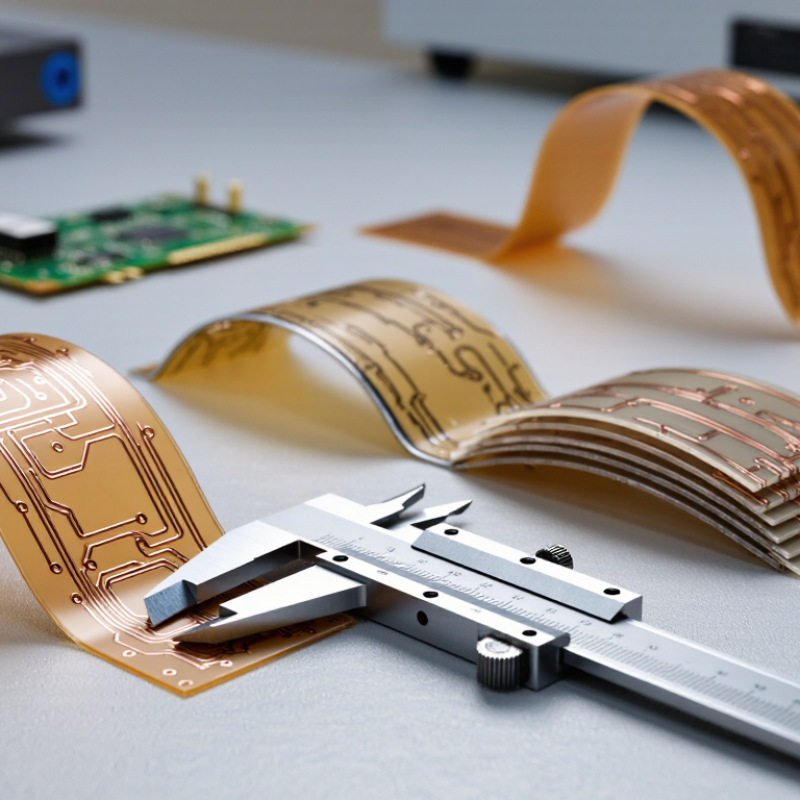
Flexible PCB boards are classified mainly by their copper-layer structure: single-sided, double-sided, and multilayer. A single-sided board places copper on one side of a flexible dielectric film. It suits simple circuits, such as a short connection between sensors and a compact display. Double-sided boards use copper on both sides, joined through plated vias. More routing space helps, but tight bends need careful placement of vias and components.
Multilayer flex boards bond three or more copper layers with insulating films and adhesive. They can carry dense signals through a small hinge or camera module, though extra layers increase thickness and make repeated bending more demanding. IPC-2223, the industry design standard for flexible printed boards, offers guidance on bend regions and construction choices. The categories look tidy on paper; real stack-ups are less tidy.
Rigid-flex boards combine flexible layers with rigid sections, so they are often grouped by structure rather than layer count alone. A device might use a rigid component area connected by a flex tail that folds around an enclosure. Grand View Research estimated the global flexible printed circuit board market at USD 20.65 billion in 2022, with projected growth of 10.3% annually from 2023 to 2030. That market estimate signals broad adoption, not a guarantee that every design needs more layers. For a moving hinge, a simpler stack may last longer. Designers still need to verify bend radius against the finished stack-up.
Single-Sided Flexible PCBs and Their Basic Construction
What Are the Top Types of Flexible PCB Boards?
Single-Sided Flexible PCBs and Their Basic Construction
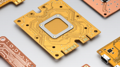
A single-sided flexible PCB has one conductive copper layer bonded to a flexible insulating film, commonly polyimide. The copper is patterned into traces and connection pads, then protected by a coverlay, typically a polymer film with adhesive. Small openings expose pads for soldering or connectors. Simple construction.
During fabrication, the copper is etched to form the circuit pattern. The coverlay is laminated over the traces, while exposed contact areas remain accessible. A designer may add local stiffeners beneath connectors to support assembly. These stiffeners do not add another circuit layer. They do add thickness, so their position matters.
Grand View Research estimated the global flexible printed circuit board market at USD 18.3 billion in 2023 and forecast a 10.1% compound annual growth rate from 2024 to 2030. This is a market estimate, not a measure of single-sided boards alone. Still, it reflects broad demand for compact, bendable circuits. In practice, a single-sided design suits simple signal paths, but repeated bending can fatigue copper. Trace direction, bend radius, and material selection deserve careful review. One detail is easy to underestimate: a board that bends during installation may not tolerate constant movement in service.
Double-Sided Flexible PCBs with Two Conductive Layers
A double-sided flexible PCB carries copper traces on both sides of a thin insulating film, often polyimide. Small plated through-holes connect the layers, letting signals cross the board without long detours. The result is more routing space than a single-sided design, while the circuit can still fold into a compact device. Two layers, one flexible assembly.
In practice, designers use this construction for camera modules, wearable sensors, and compact controls where connectors and cables take up precious room. For example, a narrow flex tail can curve around a housing, while traces on its opposite face carry separate signal paths. The extra layer can reduce board area, but it adds design and fabrication complexity. Tiny vias need careful placement, especially near areas expected to bend.
Bending deserves attention early. A board may survive installation yet fail after repeated movement if copper traces sit across a tight fold. Keeping bends gentle, limiting components in moving zones, and checking the intended bend radius can help improve reliability. Still, there is no universal safe radius; material stack-up and flexing frequency matter. This detail is easy to underestimate. A prototype should be tested in its actual enclosure, because a flat sample cannot reveal every mechanical stress.
Double-Sided Flexible PCBs: Two Conductive Layers
Double-sided flexible PCBs have two conductive layers, typically arranged on opposite sides of a flexible insulating base. For comparison, single-sided flex circuits have one conductive layer, while multilayer flex circuits have three or more; the chart shows three as the minimum for that category.
Multilayer Flexible PCBs for Dense Circuit Designs
Multilayer flexible PCBs use several copper layers separated by thin insulating films, often polyimide. This structure fits more traces into a small area, making it useful for compact cameras, medical instruments, and folding displays. Vias connect circuits between layers, while ground planes can help control electrical noise. The added layers also make the board thicker and less willing to bend. More routing space is helpful, but it is not free.
Bend requirements should guide the layer stack from the start. A board that folds once during assembly can tolerate different conditions from one that flexes thousands of times in service. Keep sharp bends away from vias and component pads, and confirm the minimum bend radius with the fabricator. Stiffeners can support connectors or components without making the entire board rigid. Even a carefully planned stack can be harder to inspect and repair, so leave room for testing access where possible.
Tips: Share the expected bend direction, radius, and cycle count with your PCB designer. Keep critical signals away from repeated bend zones. Ask for a stack-up review before routing begins; changing layer arrangements late can be frustrating.
Rigid-Flex PCBs Combining Flexible and Rigid Sections
Rigid-flex PCBs combine rigid circuit sections with flexible polyimide layers, allowing one board to fold between connected areas. Rigid zones can support components and connectors, while flexible sections route signals through narrow spaces or around a product’s internal structure. Think of a small sensor assembly: one section sits flat beneath a connector, and a flexible tail bends toward a display. Fewer separate cables may simplify assembly. But the board still needs careful mechanical design.
Bend radius matters. A fold that is too tight can strain copper traces, especially near the transition between rigid and flexible areas. Designers should also consider layer stack-up, copper thickness, adhesive, and how often the flex section moves. A bend used only during installation differs from a hinge that cycles repeatedly. That distinction is easy to underestimate. Component placement near the transition can also create stress or complicate fabrication. Clear drawings and early reviews with the fabricator help catch these issues before production. Rigid-flex is not automatically smaller or cheaper; its value depends on the device’s shape, assembly needs, and expected motion. Prototypes can reveal awkward folds that looked fine on screen.