What Is a Flexible PCB Board and How Does It Work?

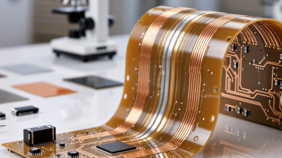
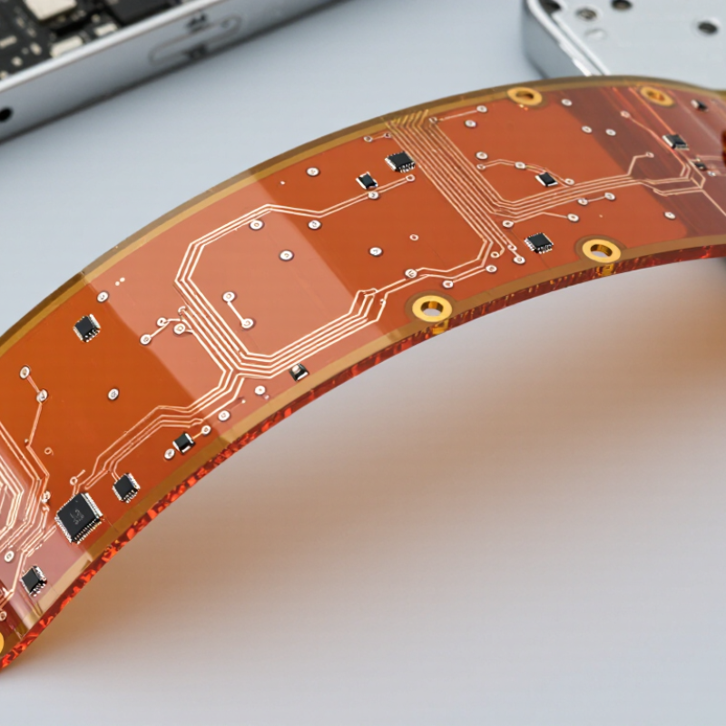
A flexible PCB board is a circuit built on a bendable insulating film rather than a rigid fiberglass panel. Thin copper traces carry signals and power between components, while a protective coverlay helps shield the circuitry. Polyimide is a common base material because it tolerates heat and repeated handling. The result can fold, curve, or fit into a narrow space. It is not simply a rigid board made thinner.

How does it work? The copper paths connect components just as they do on a conventional circuit board. The difference is that the substrate can bend within limits set by its material, thickness, and layout. A phone hinge, camera module, or compact medical instrument may use a flexible circuit to connect parts that move or sit at different angles. Fewer connectors can mean less bulk, but the circuit still needs careful routing and support. Small details matter.

Flexibility is not magic. A trace bent too sharply, or flexed too often, may crack over time. Designers therefore distinguish between circuits meant to bend during installation and those intended for repeated movement. They also consider bend radius, copper type, stiffeners, and assembly conditions. These choices affect cost and reliability, so a datasheet alone may not tell the whole story. Real performance depends on the finished design and how it is used. This guide explains the structure, operation, common applications, and practical trade-offs of a flexible pcb board, including where its advantages end.
What Is a Flexible PCB Board and How Does It Work?

Flexible PCB Boards: Definition and Core Purpose

A flexible PCB board is a circuit built on a thin, bendable insulating film, often polyimide, rather than a rigid fiberglass panel. Copper traces carry signals and power between components, while a protective coverlay helps shield the circuitry. Its core purpose is to route connections through tight spaces or moving sections without relying on bulky wires and connectors.

Electrically, a flex board works much like a rigid PCB. The difference is its structure: it can fold around a hinge, fit inside a curved housing, or connect parts that move. A small camera module, for example, may use a flex circuit to link its sensor to the main board. Not every flexible PCB is meant to bend repeatedly. That distinction matters. Repeated motion requires careful control of bend radius, copper layout, and material selection. A common design miss is treating the bend radius as an afterthought.

Tips: Check where and how often the board will flex before choosing its construction. Keep sharp folds away from components and solder joints. If the circuit moves during use, test a physical sample through repeated bends; calculations alone can miss real assembly stresses. Flex boards save space, but they are not automatically the simplest option.

Materials and Layer Structure of a Flexible PCB

A flexible PCB uses a thin insulating film instead of a rigid fiberglass core. Polyimide is common because it tolerates heat and repeated bending. Polyester may suit simpler, lower-temperature designs. Thin, but not fragile. The choice depends on the bend cycle, operating temperature, and available space.

Copper foil forms the conductive traces. Rolled-annealed copper is often selected for dynamic bends because it can better withstand repeated flexing; electrodeposited copper may suit areas that bend less. A single-layer circuit has copper on one side of the film. Double-sided designs add copper on both sides, with plated vias connecting them. Multilayer versions use bonded copper-and-film layers, but each added layer can make bending more difficult.

A protective coverlay usually places polyimide film and adhesive over the traces, leaving pads exposed for connections. Some designs use a flexible solder mask instead, though its behavior depends on the application. Adhesiveless laminates can reduce thickness and improve dimensional stability. Small details matter. Adhesive thickness, copper placement, and trace shape all affect fatigue life. Designers sometimes treat the stackup as a material list; that misses how the layers move together. Even a carefully chosen stack can fail if its bend radius is too tight. During layout, the actual motion and support points deserve close attention.

How Electrical Signals Travel Through a Flexible PCB

A flexible PCB carries signals through patterned copper traces supported by a thin dielectric film, often polyimide. A driver changes voltage at one end, creating an electromagnetic field that propagates along the trace. The electrons themselves do not race from end to end. Not quite. The signal’s return current usually follows a nearby ground or reference conductor, forming a transmission line. Trace width, copper thickness, dielectric properties, and spacing all affect impedance and timing. A sharp bend or abrupt change in geometry can disturb that impedance, causing reflections that blur fast signal edges.

Bending changes the physical geometry, but it does not make a signal travel by a different mechanism. IPC-2223C guidance commonly cites static bend radii of about six times the board thickness for single-sided flex and twelve times for double-sided flex. These are design guidelines, not guarantees for every material or repeated-motion application. Dynamic flexing needs additional care: copper near the bend can fatigue, and signal quality may drift over time. That detail is easy to underestimate. NIST’s copper data gives electrical conductivity near 5.8 × 10⁷ siemens per meter at 20°C; conductivity helps limit trace loss, but it cannot compensate for poor routing or a badly controlled return path. The useful design question is not only whether the board bends, but whether its signal path stays consistent while it does.

How Flexible Circuits Bend Without Losing Function

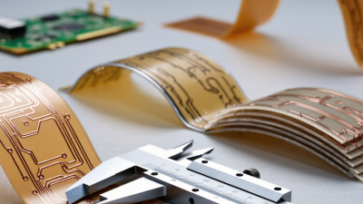
A flexible PCB bends because its thin polymer base can curve while patterned copper carries signals through the bend. The key is controlling strain. Copper placed near the board’s neutral axis stretches less, while rounded trace corners reduce stress concentration. Layer count matters, too: extra copper and adhesive can make a circuit stiffer.

IPC-2223E, the industry design standard for flexible and rigid-flex boards, treats bend radius as dependent on construction and use. Common IPC-based design guidance starts near six times the circuit thickness for a single-layer static bend, and twelve times for a double-layer bend. Repeated motion generally needs a larger radius, often around twenty times thickness for single-layer circuits. These are starting points, not guarantees. A tight crease beside a connector can still crack copper. Test the actual stack-up under its expected motion. Real assemblies are messier than drawings. A cable may rub a housing, or a bend may shift during installation. Engineers should inspect traces after cycling and avoid placing vias or solder joints in moving zones.

What Is a Flexible PCB Board and How Does It Work? — How Flexible Circuits Bend Without Losing Function

Dimension Typical Construction or Range How It Works Design Consideration
Base dielectric Polyimide film is commonly used; film thickness is often about 12.5–50 µm. The insulating film supports the copper traces while allowing the circuit to flex. Choose material and thickness for the required temperature, flexibility, and assembly process.
Conductive layer Rolled-annealed or electrodeposited copper; common copper thicknesses include approximately 12–35 µm. Copper traces carry electrical signals and power between components or connectors. Rolled-annealed copper is often preferred for repeated flexing. Trace width and copper thickness also affect current capacity and resistance.
Protective coverlay Typically a polyimide cover film bonded over the traces with adhesive; coverlay films are often around 12.5–25 µm thick. The coverlay insulates and protects copper from abrasion, moisture, and handling. Openings are required at pads and other connection areas. Coverlay and adhesive add to the circuit’s total thickness.
Common layer count Single-layer, double-layer, and multilayer flexible circuits are available. Additional copper layers allow more routing, with dielectric layers separating the conductors. More layers generally increase thickness and stiffness, so the stack-up should be kept as simple as the design allows.
Overall thickness Many flex circuits are roughly 0.1–0.3 mm thick, though the finished thickness varies by stack-up and component areas. A thinner flexible section can bend more easily than a thicker one made from similar materials. Specify thickness for the bend zone separately when stiffeners, connectors, or component pads make other areas thicker.
Static bend A circuit is bent during installation or assembly and remains in that position. Once positioned, the flex section does not undergo frequent movement. A preliminary design guideline is a bend radius of at least about 6 times the finished flex thickness; the required value depends on the material and stack-up.
Dynamic bend A circuit repeatedly flexes during normal operation. Repeated movement places cyclic mechanical strain on copper and dielectric layers. Dynamic applications typically need a larger radius than static bends; a preliminary guideline is about 20 times the flex thickness or more. Validate the design for the intended cycle life.
Trace routing in bend zones Traces are generally routed smoothly through the bend area, with curved or rounded transitions. Smoother routing helps reduce local strain concentrations as the circuit bends. Avoid sharp corners, abrupt width changes, and unnecessary vias in frequently flexed regions. Follow the fabricator’s design rules.
Component placement Components are commonly placed on rigid or stiffened regions rather than on the active bend area. Keeping components out of the bend zone reduces mechanical stress on solder joints and component bodies. Use a stiffener where support is needed for component mounting or connector insertion; a stiffener does not make that area flexible.
Why electrical function is maintained Insulated copper traces remain connected across the flexible substrate. The circuit bends as a layered structure while its conductors continue to carry signals and power. Reliable operation depends on bend radius, copper type, stack-up, trace layout, and the number of flex cycles.

Note: Values are typical design references, not universal limits. Confirm bend-radius and cycle-life requirements with the circuit fabricator for the specific material stack-up and application.

Common Types and Applications of Flexible PCBs

A flexible PCB uses copper traces on a bendable insulating film, often polyimide, instead of a rigid board. Common types include single-sided, double-sided, multilayer, and rigid-flex constructions. Single-sided circuits suit simple connections in tight spaces. Double-sided designs route signals on both faces, while multilayer versions support denser routing. Rigid-flex boards join flexible sections to rigid areas. Fewer cables.

That structure helps designers fit electronics around moving or curved parts. Wearables use flexible circuits near curved housings and small batteries. In vehicles, they can connect sensors and controls where wiring space is limited. Medical devices may use them in compact monitoring equipment, though cleaning and repeated bending require careful design. IPC-2223 provides design guidance for flexible and rigid-flex printed boards; engineers still need to check bend radius, copper thickness, and expected flex cycles for each product. Grand View Research estimated the global flexible printed circuit board market at USD 20.7 billion in 2023, forecasting a 10.4% compound annual growth rate from 2024 to 2030. A forecast is not a guarantee. Cameras, phones, and wearables are among the applications supporting demand, but market growth does not remove practical trade-offs: a thinner circuit may bend more easily, yet can be harder to assemble and protect.

What Is a Flexible PCB Board and How Does It Work?

Common Types and Applications of Flexible PCBs

Flexible PCBs use conductive copper layers on bendable insulating films. Single-sided boards have one copper layer, double-sided boards have two, and multilayer boards have three or more. The four-layer value shown here is an example, not a limit. These constructions are used in applications such as wearables, cameras, medical devices, and compact electronics.