What Is a PCB Circuit Board and How Does It Work?

A pcb circuit board is the quiet foundation beneath nearly every modern electronic device. It carries components, guides electrical signals, and provides mechanical support inside phones, vehicles, medical equipment, and industrial controls. At its simplest, it is a carefully engineered map of copper pathways on insulating material. The board does not “think.” It connects the parts that do.

PCB pioneer Dr. Paul Eisler described the printed circuit as “a means of interconnecting electrical components.” That concise idea still explains its core function. Copper traces act like controlled roads for current, while vias connect different layers through tiny drilled holes. Solder joints secure components to precise pads. Small details matter. A weak joint can stop an entire product.

Industry data shows why this technology deserves closer attention. Grand View Research valued the global printed circuit board market at approximately USD 89 billion in 2023, with continued growth expected through 2030. The IPC 2024 Global Sentiment of the Electronics Industry report also identified demand, technology investment, and supply-chain resilience as major industry concerns. These reports describe a strong market, but growth alone does not guarantee quality.

Design mistakes remain expensive. Excess heat, signal interference, poor material selection, and inadequate testing can all reduce reliability. This guide examines what a pcb circuit board is, how current travels across it, and why manufacturing choices affect performance. Some explanations will simplify complex engineering. That limitation matters. Real boards are more demanding than diagrams suggest.
What Is a PCB Circuit Board and How Does It Work?

PCB Circuit Boards: Definition, Purpose, and Basic Structure

What Is a PCB Circuit Board and How Does It Work?

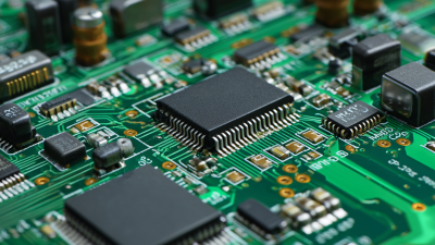
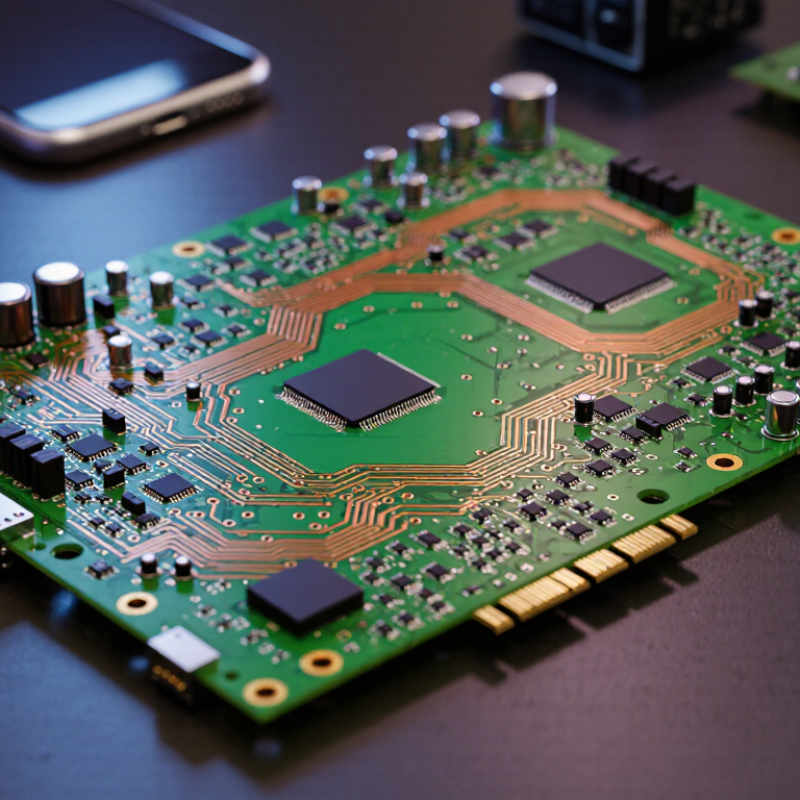
PCB circuit boards are flat platforms that connect and support electronic components. PCB means printed circuit board. Its main purpose is to carry electrical signals through carefully designed copper paths. These paths replace much of the loose wiring found in older equipment.

The global PCB market was valued at about USD 89.7 billion in 2023, according to a 2024 industry market report. Demand continues to rise with connected devices, vehicles, medical equipment, and industrial controls. A PCB may look simple. It is not. A small board can contain several signal layers, power planes, drilled holes, and controlled-impedance traces.

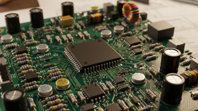
Its basic structure includes a substrate, copper foil, solder mask, and silkscreen. The substrate provides mechanical strength, often using glass-reinforced epoxy. Copper layers form conductive routes between components. Vias connect different layers through tiny drilled holes. The solder mask protects copper from oxidation and accidental solder bridges. The silkscreen adds reference labels, such as “R1” or “C3,” for assembly and inspection.

During operation, components receive power through copper planes or traces. Signals then travel between chips, sensors, connectors, and other circuits. Trace width, spacing, and length affect heat, resistance, and signal quality. Designers must also consider vibration, moisture, and manufacturing tolerances. Small errors matter. In practice, even a clean schematic can produce a difficult board when routing space becomes limited. IPC design standards provide useful guidance, but engineers still need testing, measurement, and revision. According to industry reliability studies, thermal cycling and vibration remain important causes of field failures.

The Main Layers and Materials Used in a PCB

What Is a PCB Circuit Board and How Does It Work?

The Main Layers and Materials Used in a PCB

A PCB is a flat platform that connects electronic components through controlled copper paths. Its layered structure carries power, signals, and mechanical support. The core material is usually fiberglass reinforced with epoxy resin. This rigid sheet provides strength and electrical insulation. Copper foil is bonded to its surfaces. Etching removes unwanted copper and leaves precise tracks, pads, and conductive areas.

Many boards contain several copper layers. Inner layers can distribute ground and power beneath the visible surface. Prepreg, a resin-rich fiberglass sheet, separates these copper layers. Heat and pressure bond the stack into one compact panel. Vias pass through selected layers and connect electrical paths vertically. A tiny drilled hole may link a surface pad to an internal plane. Accuracy matters here; a small alignment error can interrupt an entire circuit.

The outer copper receives a protective surface finish before components are attached. Solder mask covers most exposed copper and helps prevent accidental bridges between nearby pads. It often appears green, but color does not determine performance. Silkscreen adds reference marks, polarity signs, and part numbers for assembly and inspection. During practical troubleshooting, burned mask, lifted pads, or darkened copper can reveal overheating. Yet visual checks are imperfect. A board may look clean while hidden moisture weakens insulation. Designers must balance layer count, thickness, heat flow, signal spacing, and manufacturing tolerance. More layers can improve routing, but they also increase cost and inspection difficulty.

What Is a PCB Circuit Board and How Does It Work?

A printed circuit board (PCB) mechanically supports electronic components and electrically connects them through patterned copper traces, vias, and pads. The chart below shows a representative 1.6 mm, four-layer PCB stack-up using common FR-4 dielectric material and 1 oz copper layers.

How the layers work: Copper layers carry electrical signals and power, while the FR-4 core and prepreg electrically insulate adjacent copper layers and provide mechanical strength. Vias can connect traces between different copper layers.

How Electrical Signals Travel Through a Circuit Board

A PCB circuit board guides electrical signals through copper traces, planes, vias, and components. The signal does not simply jump from one component to another. It travels with a return current through the power or ground structure. This path forms an electromagnetic field around the trace. At low frequencies, designers often focus on resistance. At higher speeds, impedance, trace length, capacitance, and signal reflections become equally important. The IPC 2023 PCB Technology Roadmap identifies signal integrity and higher-speed interconnects as continuing design pressures.

Copper carries current efficiently. The International Annealed Copper Standard gives copper a conductivity of 100% IACS at 20°C. However, thin traces still lose energy through resistance and heat. A sharp corner, an unplanned via, or a broken return path can create noise. The effect may appear as ringing at the receiver. It may also increase electromagnetic interference. The global PCB market reached about 89.7 billion dollars in 2023, according to Fortune Business Insights, showing the scale of this engineering challenge. Market size alone does not guarantee reliable design.

Tips: Keep high-speed traces short and continuous. Route their return paths directly beneath them. Use controlled impedance when edge rates are fast. Place bypass capacitors close to power pins. Check the manufacturer’s layer stackup before routing. Simulation helps, but it is not perfect. Real boards often behave differently because materials, connectors, and assembly tolerances vary. Testing with an oscilloscope can reveal details that software misses.

The Manufacturing Process from Design to Finished PCB

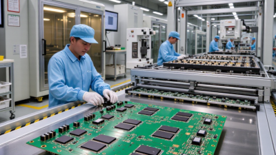
A PCB, or printed circuit board, is the physical platform that connects electronic components. Its manufacturing process begins with a digital circuit design. Engineers arrange copper traces, holes, pads, and component locations in specialized design software. They also check electrical spacing, heat paths, and signal integrity. A small layout mistake can become an expensive production problem.

The approved design moves into a design-for-manufacturing review. Fabricators check whether trace widths, hole sizes, and layer alignment suit the chosen materials. The circuit pattern is transferred onto copper-clad laminate using imaging and controlled chemical etching. Unwanted copper is removed. The remaining copper forms the electrical pathways. Multilayer boards require careful lamination, where heat and pressure bond several patterned layers together. Registration must be precise.

Next, machines drill component and via holes through the panel. Plating adds conductive copper inside these holes and across exposed surfaces. A solder mask protects selected areas, while printed markings identify component positions. The panel is then cut into individual boards. Automated optical inspection checks trace shapes and surface defects. Electrical testing verifies continuity and isolation between circuits. A board may look perfect and still fail under real heat or vibration. That is why sampling, process records, and final inspection matter. Manufacturing teams often revise designs after testing; a drawing can be technically correct but still difficult to assemble reliably.

What Is a PCB Circuit Board and How Does It Work? - The Manufacturing Process from Design to Finished PCB

Process Stage What Happens Typical Materials or Inputs Key Parameters Quality Objective
1. Electrical Design The circuit is converted into a schematic that defines components, electrical connections, power rails, and signal paths. Schematic symbols, component specifications, circuit requirements, and design rules. Voltage and current limits, impedance requirements, spacing rules, and component tolerances. A complete and electrically correct circuit definition.
2. PCB Layout Components are arranged on the board, and copper traces, vias, pads, and planes are routed between them. Layout files, footprints, copper layers, solder pads, and plated or non-plated vias. Board outline, trace width, copper weight, layer count, clearance, and controlled impedance. Reliable signal integrity, thermal performance, and manufacturability.
3. Design Rule Check Software checks the layout for shorts, unconnected nets, insufficient clearances, incorrect footprints, and manufacturing violations. Manufacturing design rules, electrical constraints, drill data, and fabrication drawings. Minimum trace and space, minimum hole diameter, annular ring, edge clearance, and layer registration. Early detection of errors before fabrication begins.
4. Material Preparation The laminate and copper foil are selected and cut according to the required board structure. Copper-clad laminate, resin-coated materials, prepreg, copper foil, and stiffeners when required. Dielectric thickness, copper thickness, glass-transition temperature, and dimensional stability. A stable material stack-up suitable for electrical, mechanical, and thermal requirements.
5. Inner-Layer Imaging A photoresist pattern transfers the inner-layer circuit image onto copper-coated laminate. Dry-film photoresist, artwork data, copper-clad cores, and ultraviolet exposure equipment. Line width, line spacing, exposure energy, and registration accuracy. Accurate reproduction of the intended copper pattern.
6. Etching and Resist Stripping Unprotected copper is chemically removed, leaving the required inner-layer traces and planes. Etching chemistry, rinsing systems, and photoresist stripping chemicals. Etch rate, undercut, conductor width, conductor spacing, and copper thickness. Clean, dimensionally accurate copper features without unwanted shorts.
7. Layer Inspection and Lamination Inner layers are inspected, aligned with insulating sheets and copper foil, and pressed under heat and pressure into a multilayer panel. Core laminates, prepreg, copper foil, alignment targets, heat, and pressure. Press temperature, pressure profile, resin flow, layer registration, and finished thickness. A void-free, mechanically stable stack-up with accurately aligned layers.
8. Drilling Through-holes and, when required, blind or buried vias are drilled to connect selected conductive layers. CNC drilling equipment, carbide drill bits, drill files, and registration targets. Finished hole diameter, drill tolerance, aspect ratio, hole position, and wall quality. Precisely positioned holes with clean walls and acceptable dimensional tolerance.
9. Electroless Copper and Plating A thin conductive copper layer is deposited on hole walls, followed by electroplating to build copper thickness. Catalytic treatment, electroless copper, electroplating baths, and plating resist. Hole-wall coverage, plating thickness, current density, bath chemistry, and uniformity. Low-resistance electrical connections between conductive layers.
10. Outer-Layer Imaging and Etching The outer copper pattern is exposed, plated as needed, etched, and stripped to form the final external circuitry. Photoresist, copper plating, etching chemistry, and outer-layer circuit data. Trace geometry, pad dimensions, annular ring, copper thickness, and registration. Accurate external conductors and dependable solderable pads.
11. Solder Mask Application A polymer coating covers most copper areas while openings remain over pads, test points, and other required locations. Liquid or dry-film solder mask, imaging artwork, and ultraviolet curing equipment. Mask thickness, pad opening size, alignment, curing conditions, and insulation resistance. Protection against oxidation, contamination, and solder bridging.
12. Surface Finish An appropriate finish is applied to exposed copper pads to improve solderability and protect the surface during storage. Protective metallic or chemical surface-finish materials. Finish thickness, flatness, shelf life, solderability, and contact requirements. Clean, flat, oxidation-resistant surfaces suitable for assembly.
13. Routing and Profiling Panels are separated into individual boards, or shaped using routed edges, V-grooves, slots, and cutouts. CNC routers, profiling tools, V-groove cutters, and mechanical drawing data. Board dimensions, edge tolerance, corner radius, slot dimensions, and tooling clearance. Accurate board shape without damaging traces, pads, or plated holes.
14. Electrical and Visual Testing The finished board is inspected for dimensions, surface defects, open circuits, short circuits, and other specified faults. Automated optical inspection, electrical test equipment, microscopes, and inspection drawings. Continuity, isolation resistance, dimensional tolerance, registration, and cosmetic acceptance criteria. Verification that the board conforms to design and manufacturing requirements.
15. Final PCB The completed bare PCB is cleaned, marked, packaged, and prepared for component assembly or direct integration into an electronic product. Finished PCB, identification markings, protective packaging, and inspection records. Board thickness, layer count, copper weight, hole structure, surface finish, and test status. A mechanically sound and electrically reliable platform for mounting electronic components.
How a PCB Works: Copper traces carry electrical signals and power between components, while vias connect selected copper layers. The insulating substrate provides mechanical support, copper planes distribute power or ground, and the solder mask helps prevent accidental electrical bridges during assembly.

Common PCB Types, Applications, and Design Considerations

A PCB, or printed circuit board, connects electronic components through copper traces.

It replaces many loose wires with controlled pathways. Power and signals travel across these traces, while vias connect layers through drilled holes. The substrate provides mechanical support, and the solder mask protects exposed copper from contamination and accidental contact. In practice, a clear layout makes testing and repairs much easier.

Common PCB types include single-layer, double-layer, and multilayer boards.

Single-layer boards suit simple controls, lighting devices, and basic sensors. Double-layer boards support denser circuits and appear in household equipment and industrial instruments. Multilayer boards handle complex computing, communication, and medical systems. Flexible boards bend inside compact products, while rigid-flex designs combine movement with structural strength. Each type has trade-offs in cost, durability, assembly, and repair.

Design decisions should begin with current, voltage, heat, and available space.

Wider traces usually carry more current and reduce heating. Sensitive signal paths need careful routing away from noisy power sections. Ground planes can improve stability, but poor layer planning may increase unwanted interference. Component spacing also affects soldering and inspection. A first layout can look excellent and still fail during thermal testing. That is where practical review matters.

Designers should check clearances, drill sizes, material limits, and manufacturing tolerances before production. Do not trust appearance alone. A small overlooked via or narrow trace can create a costly fault.