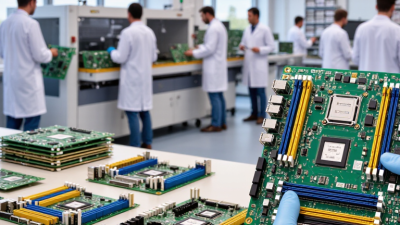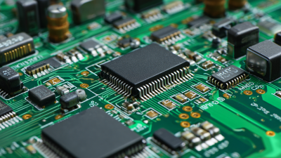
What Is Circuit Board Production?

Circuit board production turns an electrical design into a physical platform that connects and supports components. It combines material selection, imaging, etching, drilling, plating, solder-mask application, and electrical testing. Each step leaves evidence: copper traces beneath a green mask, tiny plated holes, and measured spacing between conductors. The finished board may look simple. Its reliability is not.

Manufacturing quality expert W. Edwards Deming wrote, “Quality comes not from inspection, but from improvement of the production process.” That principle matters in circuit board production, where a late inspection cannot easily repair a misregistered layer or a weak plated connection. Process controls help teams catch variation earlier, from laminate handling to drill accuracy and final continuity checks. Small details count. A dusty surface or a slight temperature shift can affect results.

This overview explains how boards move from design files to tested products, and why material choices, tolerances, and process control shape cost and performance. It also distinguishes common board types and explains where defects can arise. Production is not perfectly predictable; even a carefully managed line can produce a board that fails inspection. That deserves attention, not a claim of perfection. Understanding the process helps engineers, buyers, and product teams ask better questions before a design reaches the factory.
What Is Circuit Board Production?

What Circuit Board Production Includes

Circuit board production covers the steps that turn design files into a tested board, and sometimes a fully assembled electronic unit. Work begins with checking the layout, layer stack-up, copper thickness, and material choice. A small mismatch in the files can shift a drilled hole or leave too little space between copper tracks. It happens. A 2024 PCB industry review by Prismark estimated global production value at about $68 billion in 2023, roughly 15% below 2022. That decline reflects a cyclical market, not a change in the technical work itself.

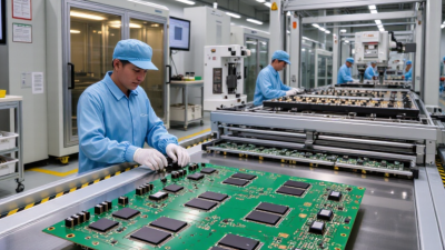
Bare-board fabrication usually involves imaging copper patterns, etching unwanted copper, drilling holes, plating connections between layers, and applying solder mask and a surface finish. Each stage needs inspection. Electrical testing checks that intended connections conduct and isolated tracks do not. Small defects matter. If assembly is included, components are placed on the board and soldered, then inspected for alignment, weak joints, or bridging. Automated optical inspection can catch visible issues, while electrical tests assess function. IPC’s electronics assembly standards describe inspection and acceptance criteria, but production plans still vary with board complexity and end use. A simple sensor board and a dense multilayer control board do not need identical checks. Even experienced teams can overlook unclear handoffs between design and fabrication; that deserves a second review.

Materials and Design Preparation

Circuit board production begins long before copper is etched. Material choices shape heat handling, signal behavior, cost, and reliability. A common rigid board uses a glass-reinforced epoxy laminate with copper foil, while flexible designs use bendable films. Engineers compare board thickness, copper weight, operating temperature, and expected service life. A board inside a warm enclosure may need different materials from one used in a handheld sensor. Small details matter.

Tips: Confirm the material stack-up before routing. Check component footprints against datasheets, not just library symbols. Leave room for mounting holes, connectors, and test points. Run design-rule checks, then inspect clearances and copper balance manually. Automated checks help, but they may miss an awkward assembly choice.

Preparation also means setting layer count, trace widths, spacing, and via sizes. These values depend on current, voltage, manufacturing capability, and signal speed. Send fabrication files with a clear layer map and revision notes. A missing drill note can cause delays. Review files as a fabricator would: can every feature be identified without guessing? Even careful layouts contain assumptions that may prove wrong, so record them and revisit them after prototypes.

How Board Layers and Circuit Paths Are Made

What Is Circuit Board Production?
How Board Layers and Circuit Paths Are Made

A circuit board’s layers are planned before production begins. The design specifies copper paths, component locations, and connections between layers. A simple board may use one or two copper layers; complex designs can contain many. Insulating material separates the copper sheets and helps support the finished board. Small details matter.

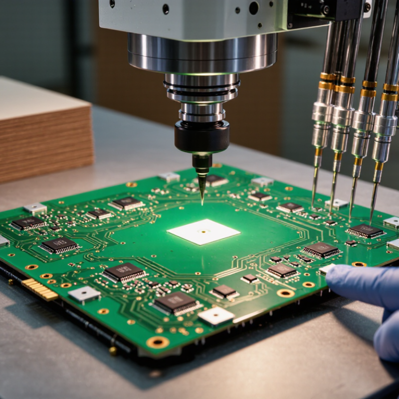
To form a circuit path, manufacturers apply a light-sensitive coating over copper. A patterned image exposes selected areas, and chemical processing removes unwanted copper. The remaining traces carry electrical signals between components. For multilayer boards, inner layers are etched, aligned, and pressed together with insulating sheets. Alignment must be exact. Small shifts can weaken connections or make later drilling miss its target.

Drilled holes allow components or layers to connect. In plated-through holes, a thin copper coating lines the hole and joins conductive layers. The board then receives its outer pattern, protective coating, and exposed contact areas. Inspection checks dimensions, continuity, and possible shorts. Even careful processes have limits: fine traces can be difficult to inspect, and material choice affects heat and strength. Designers may need to revisit a layout when test results reveal a weak path or an alignment problem.

Component Assembly and Soldering

What Is Circuit Board Production?
Component Assembly and Soldering

Component assembly places electronic parts onto a bare circuit board according to its design. Some parts sit on the surface; others have leads that pass through drilled holes. Placement machines can position tiny components quickly, while larger or unusually shaped parts may need careful manual handling. Orientation matters. A diode or integrated circuit installed backwards can prevent a board from working, even when every solder joint looks neat.

Soldering creates both an electrical connection and a physical bond. In reflow soldering, a measured amount of solder paste holds surface-mounted parts in place as the board passes through a controlled heating profile. Through-hole parts are commonly soldered with a selective or wave process, depending on the design. Temperature, cleanliness, and timing all affect the joint. Too little heat may leave a dull, weak connection; too much can damage a pad or nearby component. Small details matter.

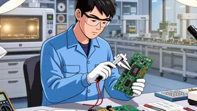
Inspection checks more than appearance. Technicians may use magnification, electrical tests, or automated optical inspection to find bridges, shifted parts, and incomplete joints. A shiny surface is not proof of a reliable connection. Even experienced teams can miss defects, so inspection methods and process settings need regular review. The work is precise, but not perfectly predictable.

What Is Circuit Board Production? - Component Assembly and Soldering

Production Stage What Happens Typical Process Controls Quality Check
PCB preparation Bare boards are checked, identified, and prepared for component assembly. Verify board revision, surface condition, and handling requirements; control moisture exposure where applicable. Visual inspection for damage, contamination, or incorrect board details.
Solder paste printing A stencil deposits solder paste onto surface-mount pads. Stencil aperture design, alignment, paste condition, and print settings are controlled. Stencil thickness is commonly around 0.10–0.15 mm, depending on the design. Solder paste inspection checks deposit position, coverage, and volume.
Component placement Automated placement equipment positions surface-mount components on the pasted pads. Placement coordinates, component orientation, polarity, and feeder setup are matched to the assembly data. Machine vision or pre-reflow inspection checks presence, alignment, and orientation.
Reflow soldering The board passes through a controlled heating profile that melts the paste and forms solder joints. Profile zones, ramp rates, peak temperature, and time above the solder alloy’s liquidus are set for the paste and components. Lead-free SAC305 solder has a liquidus temperature of about 217°C; the required profile varies by assembly. Automated optical inspection checks visible joints and component placement; X-ray inspection can assess hidden joints such as many bottom-terminated packages.
Through-hole insertion Leaded components are inserted into plated holes, either manually or with insertion equipment. Component value, orientation, lead forming, and seating are checked against assembly instructions. Visual checks confirm component position, polarity, and lead condition before soldering.
Through-hole soldering Leads are soldered to plated holes, commonly by selective soldering, wave soldering, or hand soldering. Preheat, flux application, solder temperature, contact time, and board travel are controlled according to the method and assembly requirements. Inspect for incomplete fill, bridges, insufficient wetting, and other solder-joint defects.
Cleaning and finishing Process residues are removed when required, and leads or other features may be finished to specification. Cleaning method and compatibility depend on the soldering materials, flux, components, and product requirements. Check cleanliness and confirm that no residue or finishing process has damaged the assembly.
Electrical test and release The assembled board is tested before packaging or integration into a larger product. Test coverage and acceptance limits are defined by the circuit design and product requirements. May include continuity or in-circuit testing, functional testing, and final visual inspection.

Process settings are design- and material-dependent; production profiles should be validated for the specific board and components.

Inspection, Testing, and Production Controls

Inspection, testing, and production controls help keep circuit boards consistent from one manufacturing run to the next. Checks begin with incoming materials and continue through printing, component placement, soldering, and final assembly. Operators may inspect solder joints under magnification, looking for bridges, gaps, or uneven fillets. Automated optical inspection can compare board images against defined criteria. Measurement results should be recorded, not merely judged by eye. Small defects matter.

Electrical testing checks whether connections are continuous and unwanted shorts are absent. Depending on board complexity and production volume, teams may test every board or use a documented sampling plan. Functional tests can verify that a completed assembly behaves as intended under specified conditions. Test fixtures need regular checks, since worn contacts can create misleading failures. No test catches everything.

Production controls connect findings to action. Clear work instructions, approved design files, and traceable lot records help teams identify where a problem started. When defects appear, affected boards should be separated while the cause is investigated. Process data, such as soldering temperatures or placement errors, can reveal patterns before scrap rises. Yet a checklist can look complete while a measurement method remains weak. Teams should review criteria when real defects repeatedly escape inspection, and avoid changing limits without evidence.