
What Is a Rigid Flex PCB and How Does It Work?
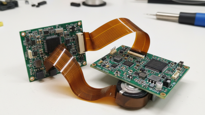
A rigid-flex PCB combines solid board sections with flexible circuitry in one connected structure. It can support components on a firm area, then bend through a narrow space like a ribbon around a hinge. This is not simply a rigid board with a loose cable attached. Copper layers, dielectric films, adhesives, and coverlays work together to carry signals while the flexible region moves. The details matter. A tight bend can strain copper, while a poorly planned layer transition can create reliability problems.
PCB design educator Rick Hartley is known for teaching careful control of signal paths and return paths. A practical application of that guidance—not a verbatim quotation—is: “Plan the electrical path as carefully as the mechanical bend.” That distinction is easy to overlook. A pcb rigid flex design must fit its enclosure, but it must also preserve electrical performance as the assembly flexes. Engineers consider bend radius, copper placement, layer stackup, component locations, and how often the board will move. They may use curved traces and keep vias away from bend zones. These choices reduce stress, though they cannot guarantee a trouble-free design.
In this guide, we’ll explain how rigid and flexible sections connect, how signals travel across them, and where common design trade-offs appear. We’ll also look at fabrication and testing, including checks for continuity and repeated-flex performance. Real assemblies rarely behave exactly like a clean diagram. Small details can matter. That is why prototypes and manufacturer feedback remain valuable before production.
What Defines a Rigid-Flex PCB?
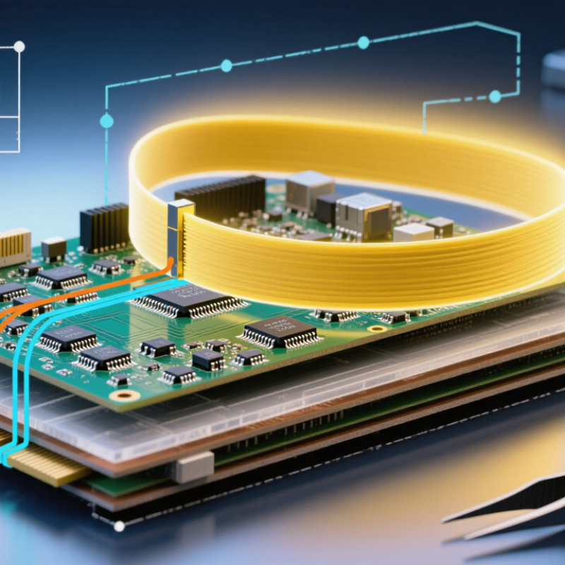
A rigid-flex PCB is defined by combining rigid circuit sections with flexible circuitry in one connected assembly. The rigid areas support components and provide stable mounting points. The flexible section bends to link them, often through a narrow passage inside a device. Unlike a cable joining separate boards, its copper traces and insulating layers form one continuous circuit structure. This integration can reduce connectors, wiring, and space, but it also makes layout and fabrication more demanding.
A typical stack uses copper conductors laminated with flexible dielectric film, often polyimide, alongside rigid layers supported by stiff materials. Coverlay protects exposed flex traces, while plated holes or other transitions connect circuit layers. The bend area needs careful design: copper type, trace direction, layer count, and bend radius all affect durability. A board may look simple on a drawing, yet repeated movement can expose weak points. Not every flexible section is meant to move during use; some bend only during assembly.
Tips: Check the specified bend radius and whether movement is static or repeated. Keep components and plated holes away from the active bend zone. Ask the fabricator to review the stack-up early. Small details matter.
What Is a Rigid-Flex PCB and How Does It Work? — What Defines a Rigid-Flex PCB?
| Dimension | What Defines It | How It Works |
|---|---|---|
| Basic structure | A single printed circuit board assembly design combines rigid circuit-board sections with flexible circuit sections. | The rigid areas support components, while the flexible areas allow the circuit to bend or fold to fit the product enclosure. |
| Rigid sections | These sections use rigid insulating materials, commonly glass-reinforced epoxy laminate, with patterned copper layers. | They provide stable surfaces for mounting components and help maintain the board’s shape in areas that should not flex. |
| Flexible sections | These sections are built on a bendable dielectric film, commonly polyimide, with flexible copper conductors. | They route electrical signals between rigid sections and can be shaped during assembly or product installation. |
| Layer construction | Rigid and flexible layers are arranged and laminated together according to the circuit design. | Conductive copper patterns form the electrical paths, while dielectric layers insulate conductors and separate circuit layers. |
| Electrical connections | Plated through-holes, vias, and copper traces connect conductive layers where the design requires them. | Signals and power can pass between layers and sections without needing separate cables or board-to-board connectors at every junction. |
| Mechanical role | The flexible portion is designed for a specified bend location and bending condition. | It can accommodate folding or limited movement, but repeated flexing must be considered in the design to reduce conductor fatigue. |
| Key design considerations | Important factors include bend radius, copper type and thickness, layer count, transition geometry, and component placement. | Components and vias are generally kept out of areas intended to flex, and the bend region is designed to avoid sharp creases or unnecessary stress. |
| How it differs from separate boards and cables | Rigid and flexible circuit areas are integrated into one interconnected board structure. | This integration can reduce connector count and wiring, while allowing a compact layout that follows the product’s shape. |
| Typical applications | Rigid-flex circuits are used in products where space, packaging, or internal movement makes a combined rigid and flexible circuit useful. | Examples include compact electronics, cameras, medical instruments, and aerospace or industrial equipment, depending on the product requirements. |
Related Posts
-
What Are the Top Rigid Flex Board Manufacturers in China?
-
2026 Best Rigid Flex PCB Suppliers for Global Buyers
-
How to Choose the Best Rigid Flex PCB Manufacturer?
-

How to Choose a Rigid Flex PCB Supplier in 2026?
-

10 Best Rigid Flex PCB Manufacturers for Global Buyers
-
Top Reasons to Choose PCB Rigid Flex for Your Next Electronics Project